

The end is in sight for achieving the thinnest and most flexible semiconductors possible. Researchers at Cornell have announced the creation of semiconducting films just three atoms thick, leaving them only two steps away from the theoretical limit of 2D materials.
The rest of this article is behind a paywall. Please sign in or subscribe to access the full content.Thinner semiconductors can be packed more tightly, making for smaller and potentially faster computing devices.
Ultrathin superconductors are not new. However, a product that is not much wider than it is thick is of little use. Many efforts have produced islands with the right thickness, surrounded by seas that are thicker or hold no material at all.
The real challenge is in creating a film that functions consistently over a substantial area. Indeed, the Nature paper describes this new discovery as having “wafer-scale homogeneity.”
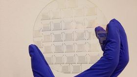
“The electrical performance of our materials was comparable to that of reported results from single crystals of molybdenum disulfide, but instead of a tiny crystal, here we have a 4-inch wafer,” said lab leader Dr Jiwoong Park.
The effect was achieved using chemical vapor deposition onto an insulating silicon oxide wafer. Both tungsten disulfide and molybdenum disulfide films were produced with remarkable 99% success rate – only two out of 200 attempts failed. The films are made by inserting the transition metal between two deposited layers of sulfur.
Credit: Ben Mills via Nature. The structure of the molybdenum disulfide layers.
“These were only the first two materials, but we want to make a whole palette of materials,” Park said.
The deposited films were also highly uniform across wafers up to 10cm across, suggesting the potential size is almost unlimited. Park's team also demonstrated that they could stack films made in this way between layers of silicon dioxide, creating what could become the thinnest multi-level electronic devices ever made.
Traditional silicon and gallium arsenide semiconductors have proved difficult to manufacture in ultrathin formats, driving the quest for materials such as the ones used here. The paper notes that transition metal disulfides have “unique electronic band structures” that provide flexibility and potential for many applications.
Some success has been achieved producing thin film semiconductors by peeling layers off crystals, but this has also been slow and inconsistent.
While the manufacturing process is currently still too slow for commercially viable mass production, the authors claim, “Our films can be used immediately for the batch fabrication of integrated circuitry consisting of FETs, photodetectors and light emitting diodes on a technologically relevant multi-inch wafer scale.” Moreover, they anticipate that the same technique will work on other substrates suitable for a variety of applications.
Single-atom layers of molybdenum disulfide were recently created using a different technique, but only on a much smaller scale.